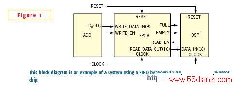
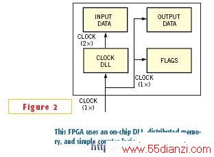
许多设计需要 FIFO 弹性缓冲器,在不同时钟速率的次系统和通道的需求中形成桥梁。然而,在某些应用中,需要FIFO缓冲器实现数据转换。一个例子是,通过FIFO缓冲器,将8位ADC连接到16位数据总线的 微处理器 (图1)。不幸地,大部分普遍使用的FIFO缓冲器不适于这个应用。本设计方案描述了为不同宽度读写数据端口的 数据宽度转换 ,怎样基于FPGA的FIFO实现共有时钟(同步)。可以使用Xilinx的Spartan II系列FPGA实现这种FIFO。这个方法使用了片上DLL(延迟锁相环)宏、分布式存储器和简单的计数器逻辑(图2)。
FIFO输入数据的宽度为8位;然而,输出数据的宽度为16位。在读写动作中只使用一个共有时钟。关键是为了使用时 钟DLL,它不只是最小化时钟脉冲相位差,还提供双倍输出的时钟频率。所以,可以实现输入数据的双重数据率,write_data_in。通过监测DLL输出时钟的样本,DLL可以补偿走线网络的延迟,有效地消除外部输入端口到设备中单独时钟负载的延迟。替代使用的阻塞存储器,本设计在FIFO中使用分布式存储器保存数据。实际上,选择阻塞存储器还是分布式存储器,依靠系统中FIFO的重要性。如果不是很关键,可以考虑使用分布式存储器。
存储器可以放在FPGA的任何位置。如果坚持使用阻塞存储器,可以简单的改变VHDL代码。可只使用一些RAM宏来替代分布式存储器。点击下载FIFO 的VHDL代码。FIFO一般使用Gray代码计数器或线性反馈移位寄存器作为读或写计数器。为实现逻辑大小的最小化,本设计只使用两个从0到7的整数和带进位的计数器。当读和写计数器相等,且进位为0时,FIFO为空。当写计数器加1等于读计数器,且进位为1时,FIFO为满。
英文原文:
Simple FIFO provides data-width conversion
Edited by Bill Travis
David Lou, Ghent University, Ghent, Belgium -- EDN, 9/26/2002
Many designs require FIFO elastIC buffers to form a bridge between subsystEMS with different cLOCk rates and aCCess requirements. However, in some applications, you need FIFO buffers for data conversion. One example is the case in which you need to connect an 8-bit ADC to a 16-bit data-bus microprocessor through a FIFO buffer (Figure 1). Unfortunately, most currently available FIFO buffers are unsuitable for this application. This Design Idea describes how to implement a common clock (synchronous version) for an FPGA-based FIFO for data-width conversion with different-width read and write data ports. You CAN implement this FIFO using a Xilinx ( www.xilinx.com ) Spartan II Series FPGA. The method uses an on-Chip DLL (delay-locked-loop) macro, distributed memories, and simple counter logic (Figure 2).
You can put the memory anywhere you like within the FPGA. If you insist on using block memory, you can eaSILy modify the VHDL code. You can just use some RAM macros to replace distributed memories. Click here to download the VHDL code for the FIFO. FIFOs commonly use Gray-code counters or linear-feedback shift registers as read or write counters. To minimize the logic size, this design uses only two integers ranging from 0 to 7 together with a carry for the counters. When the read and write counters are equal and the carry is zero, the FIFO is empty. When the write counter plus one is equal to the read counter and the carry is one, the FIFO is full.
英文原文地址: http://www.edn.com/article/CA244151.html
本文关键字:暂无联系方式DSP/FPGA技术,单片机-工控设备 - DSP/FPGA技术


