AD9516集成2.8 GHz VCO的14个输出的时钟发生器,是一种无需外部VCO的类似时钟IC,它具有超过AD9510的优点。这两款芯片都需要一个外部RC环路滤波器以构成锁相环。通过选择适合VCO和参考振荡器的最佳环路带宽可做一些性能优化以便将相位噪声造成的时钟抖动的总体影响降低到最小。广泛应用在低抖动时钟分配,为高速ADC, DAC, DDS, DDC, DUC和 MxFE提供时钟,高性能无线收发器和仪表,宽带设备和ATE.本文介绍AD9516的主要性能,方框图,应用以及评估板电路图和评估板的材料清单(BOM)。
14-Output Clock Generator with Integrated 2.8 GHz VCO AD9516-0
内置VCO基于PLL的时钟IC支持低抖动时钟应用
AD9510是一种内置锁相环(PLL)的低抖动时钟分配集成电路(IC),它可与外部压控振荡器(VCO)连接为DAC和ADC应用产生和分配一个低抖动时钟信号。AD9516是一种无需外部VCO的类似时钟IC,它具有超过AD9510的优点。这两款芯片都需要一个外部RC环路滤波器以构成锁相环。
时钟发生器的性能取决于多种因素,其中最重要的因素包括VCO的相位噪声以及参考振荡器的相位噪声和PLL的环路带宽。通过选择适合VCO和参考振荡器的最佳环路带宽可做一些性能优化以便将相位噪声造成的时钟抖动的总体影响降低到最小。
AD9510和AD9516都需要外部参考振荡器——从而使这两款器件在选择参考振荡器方面完全一样。但是,AD9510需要选择和使用一个外部VCO;虽然为满足给定频率要求可提供多种VCO,但是其中有些VCO的相位噪声特性比其它的要好。采用AD9510的时钟发生器设计允许选择能提供最高性能的VCO。
使用ADIsimPLL仿真工具显示的使用VCO(Sirenza VCO190-1455T)在1474.56 MHz处产生的491.52 MHz时钟,其中参考输入为15.36 MHz,环路带宽为100 kHz。通过对相位噪声从12 kHz到20 MHz积分计算出的该时钟发生器的等效时钟抖动为338 fs 有效值(RMS)。
AD9516有一个内置VCO,虽然它具有很好的相位噪声性能,但是在相同频率范围内它不如最好的单独VCO。尽管如此,使用AD9516可以达到非常高的时钟发生器性能。
AD9516-4在其LVPECL输出端产生491.52 MHz时钟信号的绝对相位噪声。其中VCO频率为1474.56 MHz,其环路带宽为100 kHz。参考输入频率为15.36 MHz,它采用Agilent SMA100A型信号发生器。
通过对相位噪声从12 kHz到20 MHz积分计算出的该时钟发生器的等效时钟抖动为275 fs RMS。
AD9516系列内置VCO的时钟发生器IC具有产生高质量低抖动时钟信号的能力,它解决了采用外部VCO造成的成本、尺寸和可靠性问题。
The AD9516-01 provides a multi-output clock distribution function with subpicosecond jitter performance, along with an on-chip PLL and VCO. The on-chip VCO tunes from 2.55 GHz to 2.95 GHz. Optionally, an external VCO/VCXO of up to 2.4 GHz may be used.
The AD9516-0 emphasizes low jitter and phase noise to maximize data converter performance, and can benefit other applications with demanding phase noise and jitter requirements.
The AD9516-0 features six LVPECL outputs (in three pairs); four LVDS outputs (in two pairs); and eight CMOS outputs (two per LVDS output). The LVPECL outputs operate to 1.6 GHz, the LVDS outputs operate to 800 MHz, and the CMOS outputs operate to 250 MHz.
Each pair of outputs has dividers that allow both the divide ratio and coarse delay (or phase) to be set. The range of division for the LVPECL outputs is 1 to 32. The LVDS/CMOS outputs allow a range of divisions up to a maximum of 1024.
The AD9516-0 is available in a 64-lead LFCSP and can be operated from a single 3.3 V supply. An external VCO, which requires an extended voltage range, can be accommodated by connecting the charge pump supply (VCP) to 5.5 V. A separate LVPECL power supply can be from 2.375 V to 3.6 V.
The AD9516-0 is specified for operation over the industrial range of −40°C to +85°C.
主要特性:
Low phase noise, phase-locked loop
On-chip VCO tunes from 2.55 GHz to 2.95 GHz
External VCO/VCXO to 2.4 GHz optional
One differential or two single-ended reference inputs
Reference monitoring capability
Auto and manual reference switchover/holdover modes
Autorecover from holdover
Accepts references to 250 MHz
Programmable delays in path to PFD
Digital or analog lock detect, selectable
3 pairs of 1.6 GHz LVPECL outputs
Each pair shares 1 to 32 divider with coarse phase delay
Additive output jitter 225 fS rms
Channel-to-channel skew paired outputs <10 ps
2 pairs of 800 MHz LVDS clock outputs
Each pair shares two cascaded 1 to 32 dividers with coarse phase delay
Additive output jitter 275 fS rms
Fine delay adjust (ΔT) on each LVDS output
Eight 250 MHz CMOS outputs (two per LVDS output)
Automatic synchronization of all outputs on power-up
Manual synchronization of outputs as needed
Serial control port
64-lead LFCSP
应用:
Low jitter, low phase noise clock distribution
Clocking high speed ADCs, DACs, DDSs, DDCs, DUCs, MxFEs
High performance wireless transceivers
High performance instrumentation
Broadband infrastructure
ATE 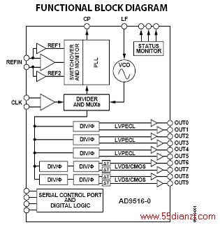
图1。AD9516方框图
AD9516评估工具
图2。AD9516评估板电路图(1)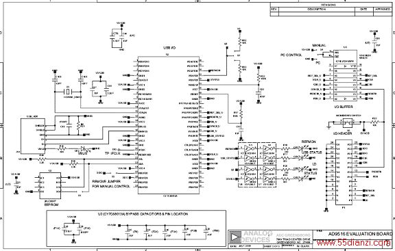
图3。AD9516评估板电路图(2)
图4。AD9516评估板电路图(3)
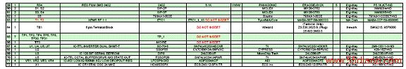
下表是AD9516评估板的材料清单(BOM)