ADI ��˾��ADL5321 ��2.3 GHz ��4.0 GHz RF�����Ŵ���������GaAs HBT�������죬����Դ5���������㷺Ӧ�������ߺ����߸���Ӧ�ã�����LTE, WiMAX, WiBro�� WLL�����Ľ���ADL5321����Ҫ���ܣ��Լ���2500 MHz-2700 MHz��3500 MHz-3850 MHzƵ�εĻ������ӵ�·��������Ԫ������ͼ�Լ���Ӧ��Ԫ���嵥��
ADL5321 2.3 GHz to 4.0 GHz RF Driver Amplifier
The ADL5321 is a broadband, linear driver RF amplifier that operates at frequencies from 2.3 GHz to 4.0 GHz. The device can be used in a wide variety of wired and wireless applications including LTE, WiMAX, WiBro, and WLL.
The ADL5321 operates with a 5V supply voltage, while only consuming 84 mA of current.
The ADL5321 is fabricated on a GaAs HBT process. The device is packaged in a low-cost SOT−89 that uses an exposed paddle for excellent thermal impedance. It operates from −40��C to +85��C, and a fully populated evaluation board is available.
With an output OIP3 of 40 dBm and output compression point of 25 dBm at 2600 MHz, the ADL5321 driver provides the highest linear output drive level for a given transmitted output power. Consuming just 84 mA, which is a 30% to 50% power savings over competing devices, the ADL5321 also features on-chip active bias circuitry, which further reduces the external component count. The driver amplifier��s Class 3A, + 4 kV, ESD (electrostatic discharge) rating also provides an exemplary degree of robustness for high volume manufacturing.
The ADL5320 is a companion part that offers lower frequency operation from 400 MHz to 2700 MHz.
��Ҫ���ԣ�
Operation from 2.3 GHz to 4.0 GHz
Gain of +14 dB at 2600 MHz
OIP3 of +40 dBm at 2600 MHz
P1dB of +25 dBm at 2600 MHz
Noise figure of 4 dB at 2600 MHz
Power supply of 5 V
Power supply current of 84 mA
Internal active biasing
Thermally efficient SOT−89 package
The ADL5320 is a 400 MHz to 2700 MHz driver
ESD rating of ��4 kV (Class 3A)
The basic connections for operating the ADL5321 are shown in Figure 8. The inputs and outputs should be ac coupled with appropriately sized capacitors. DC bias is provided to the amplifier via an inductor connected to the RF output pin. A bias voltage of 5 V is recommended.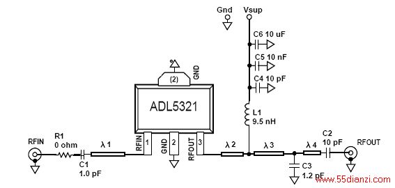
ͼ1. ADL5321��2500 MHz-2700 MHzƵ�εĻ������ӵ�·
ͼ2. ADL5321��2500 MHz-2700 MHzƵ��������Ԫ������ͼ
��1. 2500 MHz-2700 MHzƵ��ƥ��Ԫ�����
Matching Component Spacing 2500 MHz - 2700 MHz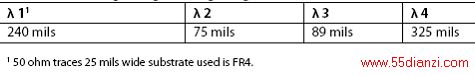
��2. 2500 MHz-2700 MHzƵ��������Ԫ���嵥
Evaluation Board Configuration Options 2500 MHz - 2700 MHz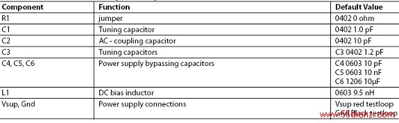
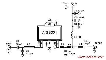
ͼ3. ADL5321��3500 MHz-3850 MHzƵ�εĻ������ӵ�·
ͼ4. ADL5321��3500 MHz-3850 MHzƵ��������Ԫ������ͼ
��3. 3500 MHz-3850 MHzƵ��ƥ��Ԫ�����
Matching Component Spacing 3500 MHz �C 3850 MHz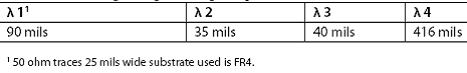
��4. 3500 MHz-3850 MHzƵ��������Ԫ���嵥
Evaluation Board Configuration Options 3500 MHz �C 3850 MHz
��Դ���е���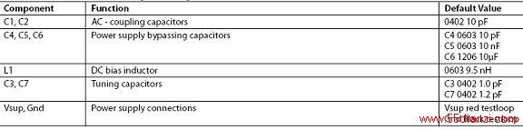
���Ĺؼ��֣�������ϵ��ʽ�繤��ժ���繤���� - �繤��ժ


