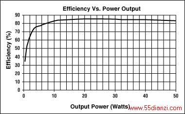
Key performance characteristics of the power supply include efficiency and output-voltage-regulation curves. Figure 9 shows the efficiency versus output power. The efficiency reaches 85% at about 25W of output power and stays relatively flat up to 50W. Even though the efficiency is very high, heatsinking is required for the power FET and output diodes. The diode will dissipate about 6W with a 10A output current, and the FET can be expected to dissipate about 3W to 4W. A slight airflow over the power supply will cool down the power transformer and the output inductor.
Figure 9. Efficiency curve.
Figure 10 shows the output-voltage regulation of the power supply from 0A to 10A of output current. Voltage measurement was done at output-voltage sense points.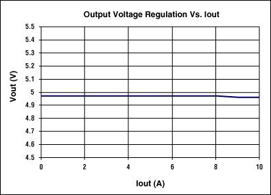
Figure 10. Output-voltage regulation.
Table 3. Power-Supply-Performance Data
Pout50WVin+36V to +72V orVin-36V to -72VVout+5VIout10AInitial Output-Voltage Set-Point Accuracy±3%*Output-Voltage Regulation Measured0.3%, over line and loadEfficiency Measured85% @ 48V and 25WInput-Output Isolation1500V for 1secSwitching TopologyFeed-forward compensated Forward Dimensions4.05" x 1.3"
*Initial set-point accuracy can be improved with external component trimming or by using a better-tolerance output-voltage sense-resistor divider.
As with any other switching power supply, component placement is very important. Because of the primary to secondary isolation, the primary and secondary grounds are separated. Figure 13 shows the separation on both sides of the PCB. The layout of the board can be changed to accommodate different footprints. In addition, the power FET and output rectifier should be mounted on a heatsink for best thermal management. In this implementation, both of these components were mounted on the noncomponent side of the board with their tabs exposed so that they could easily be mounted on a heatsink.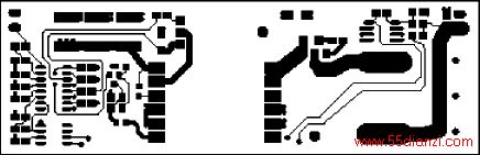
Figure 11. Top-side copper tracks of the FWD0510 power supply.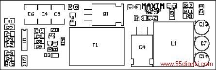
Figure 12. Component placement of the FWD0510 power supply; note that Q1 and D4 are placed on the bottom side, where their metal tabs are exposed to the heatsink plate. 
Figure 13. Bottom side copper tracks of the FWD0510 power supply.
The critical layout points are as follows:
Here, we have described the design of a 50W, telecom power supply that uses a new control IC developed specifically for this purpose. The design offers a lower-cost alternative to ready-made bricks, while providing respectable electrical performance. The circuit can be built in a relatively small area and optimized to fit a custom footprint.


