The MAX5003 controller contains an internal high-voltage preregulator that directly connects to the input voltage. Power is fed from the V+ pin into a depletion junction FET preregulator. The preregulator drops the input voltage to a level low enough to feed a first low-dropout regulator (Figure 3). The input to the LDO is brought out at the ES pin, where it is decoupled with a small ceramic capacitor. The output of the primary-side bias winding (T1-5 and T1-6) is rectified with D3 and applied to a voltage-level conditioning circuit comprised of R14, Q2, and Z1. This circuit limits the voltage to a safe level so that it can be applied to the VDD. The bias winding in this case operates in flyback mode, as opposed to the power stage that operates in forward mode. This eliminates the need for a filter inductor, reducing cost. Energy to the winding in the flyback mode is supplied by the energy stored in the magnetizing inductance of the transformer during the on time.
During initial startup, the first regulator generates the power for the VDD line, which is available externally through a corresponding pin. Forcing voltages at VDD above 10.75V disables the first LDO, turning off the high-voltage depletion FET, thus reducing power consumption by the IC especially at high input voltages. Following the VDD, the LDO is another regulator that drives VCC: It is the power bus for the internal logic, the analog circuitry, and the driver for the external power MOSFET. This regulator is needed because the VDD voltage level would be too high for the external N-channel MOSFET gate. The VCC regulator has a lockout line that shorts the N-channel MOSFET driver output to ground if the VCC LDO is not regulating. VCC feeds all circuits except the VCC lockout logic, the undervoltage lockout, and the power regulators.
A key component in any isolated power supply is the power transformer. Critical specifications of the power transformer that have a direct impact on efficiency and reliability are the primary and the secondary winding DC and AC resistances, resulting in operating losses. The AC part of the losses comes from skin and proximity effects and, depending on the transformer (whether is gapped or not), from circulating eddy currents. The proximity effect is the consequence of magnetic fields that distort the current flow in nearby winding conductors. The winding configuration plays a big role in these losses.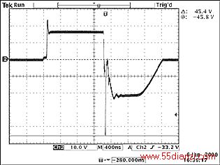
Figure 4. Waveform at transformer secondary.
Another key parameter is leakage inductance. Leakage inductance is a critical parasitic element that must be kept as low as possible to maximize power transfer to the secondary. Low leakage inductance also reduces losses in the primary. In this design, part of the leakage energy is dissipated across Q1. Figure 5 clearly shows the spike at the drain of Q1, briefly after turning off. A less critical parameter is magnetizing inductance. This is the inductance seen from the primary terminals 1 and 2 with all other terminals open-circuited. Table 2 gives the transformer specifications.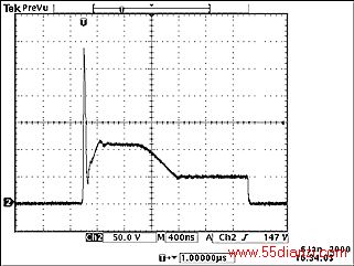
Figure 5. Q1, drain-source voltage waveform; leading-edge spike is a result of the leakage inductance energy; allowed to dissipate in Q1.
The following formula can be used to roughly calculate the energy stored in the leakage inductance and therefore dissipated in the MOSFET:![]() (8)
(8)


