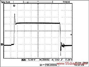
The output uses a low forward drop, dual Schottky diode, for high efficiency. This diode is rated to 20 amps with a 40V reverse breakdown voltage, adequate for this application. The total average current rectified by the diode is 10A, resulting in approximately 5.5W of power dissipation. The diode needs a heatsink capable of keeping the junction temperature at acceptable levels under worst-case ambient temperature conditions. Figure 4 shows the output voltage at the secondary of the transformer. Notice the negative-going spike on this waveform. The energy in this spike is small, and the diode is able to absorb this energy safely; in addition, the R/C network R13/C12 helps to reduce ringing at the secondary side.
Inductor L1 is capable of conducting 10A without significant losses. It is a 4.7µH high-current surface-mount type. Although it is rated for higher currents, the low series resistance helps to keep losses low. The ripple current is approximately 2.2A peak to peak. Thus, the inductor current becomes discontinuous with an output current of approximately 1.1A.
The output capacitors can be either tantalum or aluminum electrolytic types. There are three primary considerations when selecting these capacitors: allowable AC ripple-current handling, output-voltage ripple, and (as it will be seen later) control-loop stability. When using low-cost electrolytics, additional low-value ceramic capacitors can be used to further reduce switching noise spikes at the output terminals. In this circuit, the expected AC RMS current through the capacitors is in the order of 0.8A RMS; therefore, these capacitors should be sized to safely handle this level of ripple current.
The two main elements of the voltage feedback circuit are the TL431 shunt regulator and the optocoupler MOC207. Figure 6 shows the internal block diagram for the TL431. Several manufacturers produce this part, and it comes in various grades of accuracy. The internal reference voltage of the shunt regulator is 2.5V typical. An external voltage divider is used, and it consists of R11/R12 for a 5V regulated output voltage. This feedback-circuit configuration is very common in switching power supplies and is used widely. However, its operation sometimes is misunderstood, resulting in potential pitfalls. This circuit has two feedback paths from the output. One path is through the shunt regulator, providing the low-frequency gain for good output-voltage regulation, whereas the second path is through the optocoupler itself to the cathode terminal of the shunt regulator. To visualize this latter loop, it suffices to replace the shunt regulator with a virtual constant voltage source.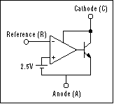
Figure 6. Simplified block diagram of the shunt regulator.
In this arrangement, any increase in output voltage will result in a higher current flowing through the LED of the optocoupler, forcing the collector voltage of the coupled phototransistor to fall and thus reduce the duty cycle. This results in a negative feedback loop that has the tendency to keep the output voltage constant. Therefore, care must be exercised when trying to stabilize this loop. The easiest method and the one adopted in this design is to rely on the ESR of the output capacitors for proper compensation of this latter feedback path. However, this puts a constraint on the minimum value of the ESR. The following formula provides a good rule of thumb for the ESR: ![]() (9) Tolerances of ±30% for the ESR should be certainly adequate. It's important to point out that by meeting equation (8) in an otherwise well-designed system, the phase margin at the unity gain crossover point of the control loop approaches 90 degrees for a excellent transient response.
(9) Tolerances of ±30% for the ESR should be certainly adequate. It's important to point out that by meeting equation (8) in an otherwise well-designed system, the phase margin at the unity gain crossover point of the control loop approaches 90 degrees for a excellent transient response.
Example: ![]() (10)
(10)
Thus, in order to get the required ripple at the output, one or more capacitors may have to be paralleled. For a 50mV peak-to-peak voltage ripple at the output, four 330µF capacitors that have an ESR of 90mΩ each can be used.
The compensation capacitor around the shunt regulator in most cases is not very critical, and its value can be around 0.1µF. Much lower values should not be used for this capacitor, as they could reduce the overall phase margin of the control loop.
The feedback circuit is completed in the primary by connecting the collector of the phototransistor in U2 to the CON input of the MAX5003. Although the control IC contains an error amplifier, that amplifier is not used in this case. However, this amplifier is very useful for non-isolated applications and in cases where regulation is done through a biasing auxiliary winding connected to the primary side.
The input circuit consisTs of three ceramic bypass capacitors, c4/c5/c6. When embedding the power supply to an actual system, it is advisable to use bulk storage capacitors. These capacitors must be sized so that they can safely handle the ripple currents present at the input of the converter.![]() (11)
(11)
where Ip is given by the following:![]() (12)
(12)
It should be noted that the worst-case ripple current through the input capacitor is around 50% duty cycle. For the circuit in Figure 1, the AC capacitor ripple current is 1.5A RMS. These capacitors should be placed very close to the input to avoid long traces from carrying high-frequency switching currents that can cause EMI problems. Additional input filtering may be necessary to meet applicable regulations.
Waveforms at key points of the circuit help explain the operation further. Figure 5 shows the drain source waveform of the switching FET. The initial spike is a result of the leakage inductance of the transformer. This is much lower at lower-output power levels. In this case, the FET absorbs the leakage energy.
Figure 7 shows the voltage pulse at the output of the secondary rectifier. This is a relatively clean waveform with minor leading- and trailing-edge spikes.