本设计方案描述了上一个方案的改进(参考文献1)。如图1中电路使用普通的 SPST 按键开关 S1代替原设计所需的SPDT开关。使用隔膜开关极大的简化了设备的工业化设计,并提高了工效。此外,电路通过未激励开关消除电流的方法,从而略微减少了现有模式中的电流消耗。
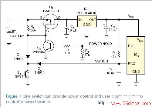
备用模式中,MOSFET Q1仍然关闭,消耗电池少于1 &mICro;A的漏电流。按下开关S1,通过二极管D1将门极拉到地,使Q1打开。电压稳压器IC1开启,为微处理器IC2供能。微处理器启动,并将P1.1输出端口置高。打开晶体管Q2,锁存系统能量到允许S1断开。与此同时,电阻R3上拉微处理器输入端口P1.2到VCC。按下开关几秒钟,通过二极管D2使P1.2输入下拉,发按键触发事件的信号到固件。完成程序以后,微处理器将输出端口P1.1置低来关闭Q2。从而,直到使用者按下S1重启程序时为止,Q1使系统掉电。
选择器件的时候,确保Q1的栅-源极击穿电压超过可能输入的最大电压;否则,使用齐纳击穿二极管来限制为Q1供电的栅-源极电压。如果电压稳压器IC1包括一个开/关控制引脚,就可以忽略Q1。为了用不同开关电源设备代替Q1
,例如NPN双极晶体管或继电器,指定Q2供给开关设备所需的控制电流。为进一步减少电路器件的数量,用适当的共阴极双二极管阵列替代二极管D1和D2,例如BAV70。如果IC2包括内置的上拉电阻,就可以忽略电阻R3,许多现代微处理器都是这样的。
英文原文:
SPST pushbutton switch combines power-control, user-input functions
One control serves multiple functions.
Eugene Kaplounovski, Vancouver, BC, CANada; Edited by Brad Thompson and Fran Granville -- EDN, 9/28/2006
This Design Idea describes an enhancement to a previous one (Reference 1). The circuit in Figure 1 uses a normally open SPST pushbutton switch, S1, instead of the SPDT switch that the original design required. You can use a membrane switch to significantly simplify the industrial design of the device and enhance its ergonomics. In addition, this circuit slightly reduces the current drain in active mode by eliminating current flow through the unactuated switch.
In standby mode, MOSFET Q1 remains off and consumes less than 1 µA of leakage current from the battery. Pressing switch S1 turns on Q1 by pulling its gate to ground through diode D1. Voltage regulator IC1 turns on and supplies power to microcontroller IC2. The microcontroller boots up and asserts its P1.1 output high, turning on transistor Q2 and latching on the system's power to allow release of S1. Meanwhile, resistor R3 pulls the microcontroller's input, P1.2, to VCC. Pressing the switch a second time pulls the microcontroller's P1.2 input low through diode D2 and signals the button-pressed event to the firmware. After completing its program, the microcontroller
When selecting components, ensure that Q1's gate-source breakdown voltage exceeds the highest possible input voltage; otherwise, use a zener diode to limit Q1's applied gate-source voltage. You CAN omit Q1 if voltage regulator IC1 includes an on/off-control PIN. To replace Q1 with a different power-switching device, such as an NPN bipolar transi stor or a relay, specify Q2 to provide the control current that the switching device requires. To further reduce the circuit's component count, replace diodes D1 and D2 with a suitable common-cathode dual-diode array, such as the BAV70. Omit resistor R3 if IC2 includes built-in pullup resistors, as do many modern microcontrollers.
Reference
Hageman, Steve, "Single switch serves dual duty in small, microcontroller-based system," EDN, March 30, 2006, pg 96.
英文原文地址: http://www.edn.com/article/CA6372827.html
上一篇:混合信号测试系统开关的优化


