飞思卡尔M1322x ZigBee PiP方案
点击数:7230 次 录入时间:03-04 11:38:04 整理:http://www.55dianzi.com 电子技术
飞思卡尔(Freescale)公司的MC13224是第三代 ZigBee封装内平台( PiP),集成了完整的低功耗2.4GHz无线电收发器,基于32位ARM7核的MCU,用于IEEE 802.15.4 MAC 和AES安全加密的硬件加速器以及MCU成套外设,是高密度低元件数的IEEE 802.15.4综合解决方案,能实现点对点连接和完整的ZigBee网状网络,因此可广泛应用在住宅区和商业自动化,工业控制,HVAC, 卫生保健和消费类电子等产品.本文介绍了MC13224的主要特性,方框图,RF无线接口以及软件特性和几种开发工具如1322x传感器参考板,1322x-NCB网络板, 1322x-LPB低功耗板和1322x-USB板的主要特性.
MC13224V Advanced ZigBee- Compliant Platform-in-Package (PiP) for the 2.4 GHz IEEE® 802.15.4 Standard The MC13224V is Freescale’s third-generation ZigBee
platform which incorporate a complete, low power, 2.4 GHz radio frequency transceiver, 32-bit ARM7 core based MCU, hardware acceleration for both the IEEE 802.15.4 MAC and AES security, and a full set of MCU peripherals into a 99-pin LGA Platform-in-Package (PiP).
The MC13224V solution can be used for wireless applications ranging from simple proprietary point-to-point connectivity to complete ZigBee mesh networking. The MC13224V is designed to provide a highly integrated, total solution, with premier processing capabilities and very low power consumption.

The MC13224V MCU resources offer superior processing power for ZigBee applications. A full 32-bit ARM7TDMI-S core operates up to 26 MHz. A 128 Kbyte FLASH memory is mirrored into a 96 Kbyte RAM for upper stack and applications software. In addition, an 80 Kbyte ROM is available for boot software, standardized IEEE 802.15.4 MAC and communications stack software. A full set of peripherals and Direct Memory Access (DMA) capability for transceiver packet data complement the processor core.
The RF radio interface provides for low cost and the high density as shown in Figure 1. An onboard balun along with a TX/RX switch allows direct connection to a single-ended 50-Ω antenna. The integrated PA provides programmable output power typically from -30 dBm to +4 dBm, and the RX LNA provides -95 dBm sensitivity. In addition, separate complementary PA outputs allow use of an external PA and/or an external LNA for extended range applications. The device also has onboard bypass capacitors and crystal load capacitors for the smallest footprint in the industry. All components are integrated into the package except the crystal and antenna.
In addition to the best-in-class MCU performance and power, the MC13224V also provides best-in-class power savings. Typical transmit or receive current is 20 mA with the CPU at 2 MHz operation and even lower with the bus stealing enabled. Onboard power supply regulation is provided for source voltages from 2.0 Vdc to 3.6 Vdc, and the source voltage can be as low as a regulated 1.8 Vdc if the non-volatile memory is powered directly from the source. Numerous low current modes are available to maximize battery life including sleep or restricted performance operation.
Applications include, but are not limited to, the following:
Residential and commercial automation
―Lighting control
―Security
―Access control
―Heating, ventilation, air-conditioning (HVAC)
―Automated meter reading (AMR)
Industrial Control
―Asset tracking and monitoring
―Homeland security
―Process management
―Environmental monitoring and control
―HVAC
―Automated meter reading
Health Care
―Patient monitoring
―Fitness monitoring
Consumer
―Remote control
―Entertainment systems
―Cellular phone attach

图1.MC13224V RF 无线接口
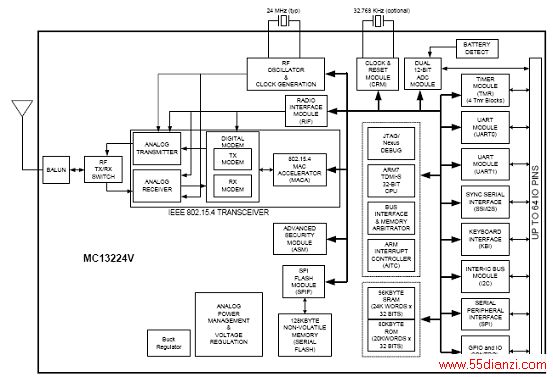
图2.MC13224V 简化方框图
主要特性:
IEEE 802.15.4 standard compliant on-chip transceiver/modem
―2.4 GHz ISM Band operation
―16 selectable channels
―Programmable transmitter output power (-30 dBm to +4 dBm typical)
―World-class receiver sensitivity
< -96 dBm typical receiver sensitivity using DCD mode (<1% PER, 20-byte packets)
< -100 dBm typical receiver sensitivity using NCD mode (<1% PER, 20-byte packets)
Hardware acceleration for IEEE 802.15.4 applications
―MAC accelerator (sequencer and DMA interface)
―Advanced encryption/decryption hardware engine (AES 128-bit)
Supports standard IEEE 802.15.4 signaling with 250 kbps data rate
32-bit ARM7TDMI-S CPU core with programmable performance up to 26 MHz (24 MHz typical)
Extensive on-board memory resources
―128 Kbyte serial FLASH memory (will be mirrored into RAM)
―96 Kbyte SRAM
―80 Kbyte ROM
Best-in-class power dissipation
―21mA typical RX current draw (DCD mode) with radio and MCU active
―28 mA typical TX current draw with radio and MCU active (coin cell capable)
―5mA maximum current draw with MCU active (radio off)
―0.9mA maximum current with MCU idle (radio off)
―1.1 μA maximum Hibernate current (retain 8 Kbyte SRAM contents)
―0.3μA maximum Off current (device in reset)
Extensive sleep mode control and variation
―Hibernate and Doze low power modes
―Programmable degree of power down
―Clock management
―Onboard 2kHz oscillator for wake-up timer.
―Optional 32.768 kHz crystal oscillator for accurate real-time sleep mode timing and wake-up with a possible sleep period greater than 36.4 hours
―Wake-up through programmable timer, external real-time interrupts, or ADC timer
Extensive MCU peripherals set
―Dedicated 802.15.4 modem/radio interface module (RIF)
―Dedicated NVM SPI interface for managing FLASH memory
―Two dedicated UART modules capable of 2Mbps with CTS/RTS support
―SPI port with programmable master and slave operation
―8-pin keyboard interface (KBI) supports up to a 4x4 matrix. Also, provides up to 4
asynchronous interrupt inputs for wake-up
―Two 12-bit analog-to-digital converters (ADCs) share 8 input channels
―Four independent 16-bit timers with PWM capability. These can cascade in combinations up to 64-bit operation
―Inter-integrated circuit (I2C) interface
―Synchronous Serial Interface (SSI) with I2S and SPI capability and FIFO data buffering
―Up to 64 programmable I/O shared by peripherals and GPIO
Powerful In-circuit debug and FLASH programming available via on-chip debug ports
―JTAG debug port
―Nexus extended feature debug port
System protection features
―Low battery detect
―Watchdog timer (COP)
―Sleep mode timer
Low external component count
―Only antenna needed for single-ended 50-Ω RF interface (balun in package)
―Only a single crystal is required for the main oscillator; programmable crystal load capacitors are on-chip
―All bypass capacitors in package
Supports single crystal reference clock source (typical 24 MHz crystal with 13 - 26 MHz usable) with on-chip programmable crystal load capacitance or external frequency source. Also provides onboard 2kHz oscillator for wake-up timing or an optional 32.768 kHz crystal for accurate low power timing.
2.0V to 3.6V operating voltage with on-chip voltage regulators; down to 1.8V with off-chip
regulation
Optional buck converter for better battery life.
-40°C to +105°C temperature range
RoHS-compliant 9.5mm x 9.5mm x 1.2mm 99-pin LGA package
[1] [2] 下一页
本文关键字:卡尔 电子技术,电工技术 - 电子技术


