Circuit Description
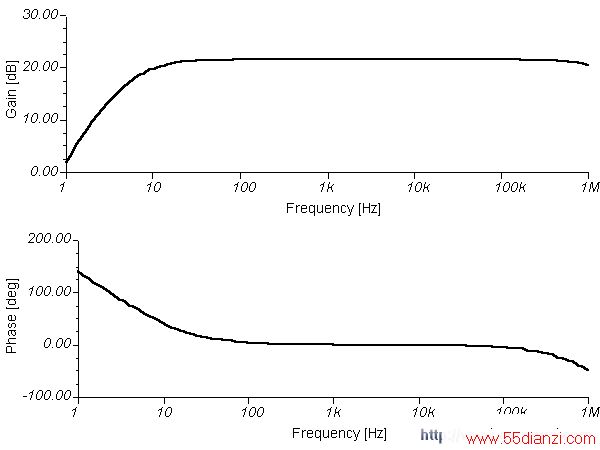
The amplifier operates in Class AB mode; the single 470R preset resistor controls the quiescent current flowing through the BD139/140 complimentary output transistors. Adjustment here, is a trade-off between low distortion and low quiescent current. TypICally, under quiescent conditions, standby current may be 15 mA rising to 150 mA with a 50 mV input signal. A simulated Frequency response is shown below:
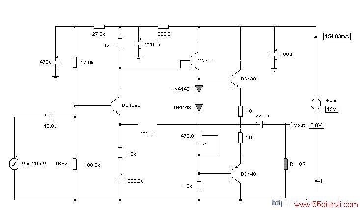
The circuit is DC biased so that the EMItters of the BD139 and BD140 are at approximately half supply voltage, to allow for a maximum output voltage swing. All four transistors are direct coupLED which ensures:-
(i) A good low frequency response
(ii) Temperature and bias change stability.
The BC109C and 2N3906 operate in common emitter. This alone will provide a very high open loop gain. The output BD139/140 pair operate in emitter follower, meeting the requirements to drive low impEDAnce speakers. Overall gain is provided by the ratio of the 22k and 1k resistor. A heat sink on the BD139/140 pair is recommended but not essential, though the transistors will run 'hot' to the touch.
本文关键字:放大器 音频功率放大-放大器,单元电路 - 音频功率放大-放大器
上一篇:D类125W低音炮功放电路


